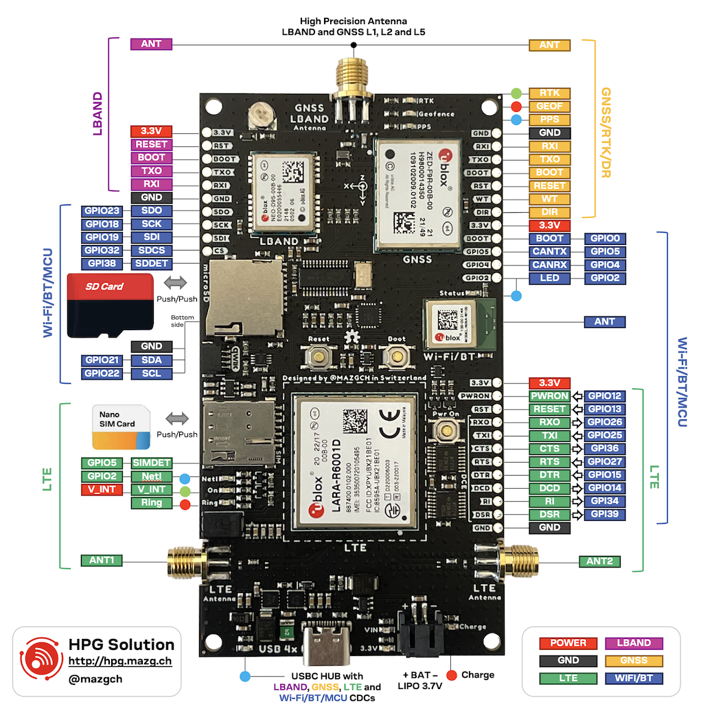
This hardware was designed with Autodesk Eagle and is hugely based on Sparkfun open-source designs. The PCB is a standard four-layer PCB 1.6mm with quite conservative design rules and components, passives are mostly 0603. The core of the circuit is centered around various u-blox modules. The design's default assembly option are the following modules.
| u-blox Module | Function |
|---|---|
| NINA-W106 | An ESP32 based WIFI and BT module with Open CPU that will host the application. |
| LARA-R6001D | A LTE Cat 1 cellular modem with 2G / 3G fallback. |
| ZED-F9R | A GNSS Module with RTK, DR and L1/L2 multiband capability. |
| NEO-D9S | A LBAND receiver to get PointPerfect correction service. |
Here you can find the schematic, layout and pictures of both sides of the PCB.


There board was designed for u-blox LARA-R6001D LTE modem, but it allows SKUs by swapping the cellular module to a SARA-R510 for LTE Cat M1 NB-IoT or a LENA-R8001 Cat 1 bis. Several different modem variants are available from u-blox, only some BOM adjustments might be needed to make different SKUs of this function board. The board requires two external LTE antennas with SMA connectors (only one antenna would be used for LENA-R8001, SARA-R510. The LTE modem uses DCE notation and signal are connected straight to the NINA CPU (no null modem, crossover). The LTE_PWR_ON pin is also connected to a button to allow manual turning on of the LTE modem. The LTE_RESET pin unfortunately does not have a pull up resistor, this could be considered as a mistake, but it can be set by the NINA CPU after software is loaded. If this is not done, then the module will turn off after it booted
| u-blox Series | LTE Standard | # Antenna |
|---|---|---|
| LARA-R6 | LTE Cat 1 with 2G / 3G fallback | 2 |
| LENA-R8 | LTE Cat 1bis with 2G / 3G fallback | 1 |
| SARA-R5 | LTE Cat M1 / NB-IoT | 1 |
| SARA-R4 | LTE Cat M1 / NB-IoT with 2G fallback | 1 |
The board was designed for u-blox ZED-F9R high precision GNSS RTK and DR module and a NEO-D9S, but it allows SKUs by swapping the modules to different variants such a ZED-F9P or the NEO-D9C that supports Japan's CLAS system. The board requires an external L1/L2/L5 and LBAND antenna with SMA connectors.
NINA-W106-01 is a ESP32 with 8MB of FLASH memory. This module is responsible to run the software of the whole design. It can be easily programmed using different environments. The RESET and BOOT pins can be controlled with buttons and as well though a special Auto Reset circuit.
| GPIO | Signal Function | DIR | Comment |
|---|---|---|---|
| 0 | BOOT / GPIO0 | IN | <- BOOT button, USB CDC RTS/CTS |
| 1 | CDC_TX | OUT | -> USB CDC RX |
| 2 | LED / GPIO2 | OUT | -> LED |
| 3 | CDC_RX | IN | -> USB CDC TX |
| 4 | GPIO4 / CAN_RX | I/O | <- CAN (external) |
| 5 | GPIO5 / CAN_TX | I/O | -> CAN (external) |
| 12 | LTE_PWR_ON | OUT | active HIGH, no pull up! |
| 13 | LTE_RESET | OUT | active LOW, ext pulled LOW |
| 14 | LTE_DCD | OUT | -> LTE. |
| 15 | LTE_DTR | OUT | -> LTE |
| 18 | MICROSD_SCK / SCK | OUT | -> SD card |
| 19 | MICROSD_SDI / COPI / MOSI | OUT | -> SD card |
| 23 | MICROSD_SDO / CIPO / MISO | IN | <- SD card |
| 21 | I2C_SDA | I/O | <-> GNSS, LBAND, LTE, QWIC |
| 22 | I2C_SCL | OUT | -> GNSS, LBAND, LTE, QWIC |
| 25 | LTE_TXI | OUT | -> LTE |
| 26 | LTE_RXO | IN | -> LTE |
| 27 | LTE_RTS | OUT | -> LTE |
| 32 | MICROSD_CS | OUT | -> SD |
| 33 | VCC_EN | OUT | -> power supply |
| 34 | LTE_RI | IN | <- LTE |
| 35 | VIN/3 | IN | <- power supply |
| 36 | LTE_CTS | IN | <- LTE |
| 37 | LTE_ON | IN | <- LTE |
| 38 | MICROSD_DET | IN | <- SD card holder |
| 39 | LTE_DSR | IN | <- LTE |
| RESET | RESET | IN | <- RESET button, USB CTS RTS/CTS |
The board has two 1A LDOs, one for the LTE modem and a second for all other functions. The status of the Power supply can be monitored using the different LEDs across the board. A changer is provided to support charging of a single 3.7V LIPO cell. A special LED will indicate the charging status. The 3.3V pins on the pin headers are output only and can be used to power an external sensor or device like a CAN transceiver.
- USB The USB-C port provides as interface to an external host and is used for supplying the board.
- CAN The GPIO4 and GPIO5 of the NINA-W106 can be used to connect a CAN transceiver such as a SN65HVD230. Thre a simple breakout board that you can attach using jumper wires such as the CJMCU-230
- BAT A 3.7V single LIPO cell can be connected and will be charged when USB is connected.
- QWIK The QWIK connector can be used to connect other I2C devices such as sensors or a display.
External antennas have to be connected to operate the device. The combined GNSS and LBAND antenna should support at least L1, L2 and LBAND frequency bands and it can support L5 band in addition. The antenna should be an antennna that is high precision capable, typically these are Helix type of antennas or active patch antennas with dual feed and reasonably sized GND planes (>10cm). If the antenna does not come with a ground plane, place it on a metal surface such as a car roof. The LTE modem needs to 4G capable antennas and cover the band of the modem usually this is 700kHz - 2.6GHz. In addition you need to insert a SIM card with a data plan from your local mobile network operator. A micro-SD card is only required if you intend to record logfiles from the modem of GNSS_
- Plexi were ordered from Alibaba Shenzhen Elemei Display Products Co., Ltd they offer laser cut custom plexi under part number OEM and ODM custom laser cut acrylic shapes customized service you send them the two PlexiTop and PlexBot layers exported as DXF file.
- LTE antennas were ordered from Advanced Aerial Store, you need 2pcs (= one order) of the following product for each board 2pcs/lot 4G Antenna 10dBi SMA Male 700-2700MHz for 4G LTE Router External Antenna
- The screws an nuts were ordered from LANHAI Fastener Store, for a single board 4pcs are needed from each part.
- The LTE_PWR_ON is floating towards GND, this causes the modem to constantly reset if no software is loaded. Software needs to be loaded that configures the GPIO12 either output HIGH or as INPUT with PULL-UP enabled. During reset the ESP applies however some LOW and high signal. It would be best to swap the LTE_RESET and LTE_PWRON pins to avoid changes during updates or reset.
- The C41 was added to the Auto Reset circuit of the NINA-W106. This sometimes can cause issues with certain terminal applications or if the BOOT GPIO is used for other functions. Simply remove the C41 with a soldering iron if it causes issues for you.
- The shield of the SIM card holder is not connected to GND in the symbol. To make SIM detection work, we have to connect it to GND by makeing a solder bridge to GND pads of C38/36. In addition the software needs to set AT+UGPIOC=42,7 and AT+UDCONF=50,1. If SIM detection is not needed and then it is better to maybe remove R50.
- On the v0.9 build some of the SIMhard holders are not porperly positioned on the board. This results in the component being a bit tilted due to the guidance pins. The parts were not repositioned but simply fixed with just more solder.
- If special firmware is loaded to ZED-F9 (e.g., dev builds), make sure that RTK_STAT assigned to GPIO11 and GEOFENCE to GPIO12 to use that function.
- Higher baud rates on the LTE are not recommended even if RTS / CTS is used, this is a software issue and unrelated to hardware.
- LENA-R8: prototype require VCC of the module to be higher than 3.5V, this can be fixed by changing the dedicated LTE LDO to a adjustable version with a resistor divider at 3.8V. Also Pin 33 USB_BOOT of LENA should be routed to a jumper that can connect to VINT (V1.8) to allo firmware update over USB.
- Pins could be reassigned, to allow use of JTAG as alternative to the full 8 wire UART (second level shifter would need to be disabled.